
Multi-die FPGA routing: circuit models and VTR architecture exploration
A VTR/VPR study evaluates 2.5D and 3D inter-die routing using circuit models and benchmarks, with gains tied to the modeled connection architecture.
Audience and applicability
For FPGA-CAD and architecture researchers. The study helps identify which physical inter-die assumptions belong in a routing experiment and which results still need validation beyond a simulated fabric.
Inter-die wires need an architecture model
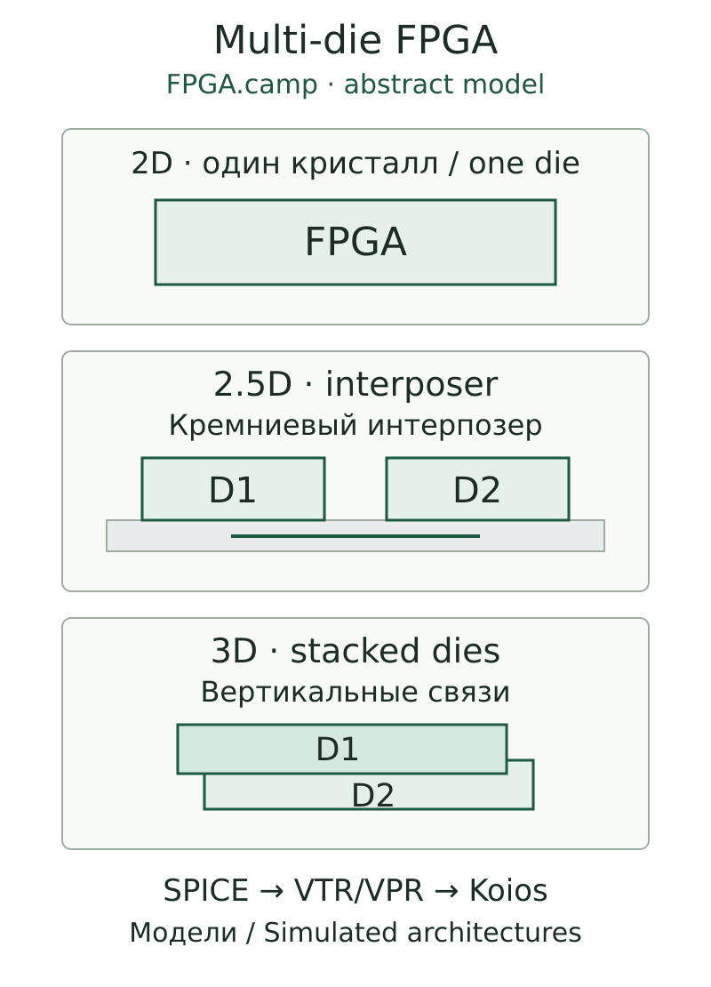
Amirhossein Poolad, Soheil Gholami Shahrouz, Andrew Boutros and Vaughn Betz extend VTR to describe routing across 2.5D interposers and 3D die stacks. VPR placement, routing and lookahead are modified alongside the routing-resource representation. Scatter/gather patterns describe how local wires reach scarce inter-die connections; CHANZ represents vertical routing explicitly.
The authors use HSPICE circuit models for active-die circuitry in a 7 nm process and a 45 nm silicon interposer. Their exploration varies connection count, fan-in/fan-out, crossing technology and interposer length. Benchmarks come from Koios, with results normalized to a 2D baseline. This is circuit/CAD modeling, not a measurement of a fabricated new FPGA.
Read the gains with their conditions
| Architecture | Wirelength relative to 2D | Critical-path delay relative to 2D | Scope |
|---|---|---|---|
| 3D: best wirelength row | 14% reduction | 4% improvement | 5 µm pitch; Nsg=12; Fg/Fsc=64/64 |
| 3D: best delay row | 8% reduction | 6% improvement | 10 µm pitch; Nsg=1; Fg/Fsc=32/32 |
| 2.5D: 32% connectivity | 2% overhead | 4% overhead | 5 µm pitch; Nsg=6; Fg/Fsc=12/16; interposer length 9 LB; α=0.32 |
Nsg denotes connection count; Fg/Fsc are gather/scatter fan-in/fan-out. The best wirelength and delay occur in different 3D configurations. Results are author-reported CAD outcomes, not board measurements.
Data sourceThe evaluated Koios subset spans roughly 12,000–759,000 primitives and fabric grids from 78×78 to 335×335. Smaller circuits are omitted: the maximum modeled interposer wire is 37 logic-block lengths, requiring a grid threshold of 74×74. The reported outcomes therefore describe this selected benchmark/size range, not every Koios circuit.
More inter-die connections do not automatically remove every cost. Their drivers and multiplexers consume area, long interposer wires add delay, and insufficient connectivity can make a circuit unroutable. Fan-in, wire length and connection density should therefore be explored together. Report designs that fail routing alongside designs that finish, rather than calculating a success-only average.
What a reproducible CAD experiment should pin
- Architecture XML, die topology, local routing channels and all inter-die parameters.
- Circuit-model assumptions, process models and delay/area extraction settings.
- VTR/VPR revision, placement/routing settings, seeds and stopping conditions.
- Benchmark revisions, the 2D baseline and failed-routing cases, with per-circuit outputs before aggregate metrics.
These are recommendations for evaluating an adaptation. The paper does not establish that the same percentages apply to a vendor device, another process model or a different workload mix. A timing result from the modeled routing graph is not a timing signoff report for a physical board.
Code, versions and figure rights
The primary source is arXiv v1 from 4 June 2026. Versions v2 and v3 appeared on 12 and 30 June. The latest text retains the headline numbers, but changes the XML example from 3D to 2.5D, clarifies earlier VTR limitations and expands the discussion of interposer routing. A reader should not mix v1 text with later figure numbers or example syntax.
The authors link the public VTR repository and say their extensions are integrated with master. We inspected tree abd1c93823b18d3de2475c2217f908bcc904a69a; it is an inspection pin, not an identified experiment revision. Most VTR code uses MIT, with separate terms for some components and benchmarks. The paper's CC BY-NC-ND 4.0 license does not establish permission for adapted source figures on this site, so the diagram is original. FPGA.camp has not repeated the routing or circuit experiments.
Sources
Full v1 architecture exploration
Intermediate version: arXiv v2
Latest compared text: arXiv v3
VTR: inspected source revision